With the continuous growth of global energy demand and the increasing awareness of environmental protection, photovoltaic power generation, as a renewable and clean energy form, has received widespread attention. Perovskite is considered to be a new material with unlimited potential in the photovoltaic field due to its excellent photoelectric conversion efficiency and low cost. It can be said to be a "rising star" in the photovoltaic industry. So, what tests are needed to improve the photoelectric conversion efficiency of perovskite cells?
Prospects of the photovoltaic industry
In 2022, China's new energy power generation installed capacity accounted for 49.5% of the total installed capacity, of which solar power generation accounted for 15.3%. Compared with 12.9% of solar power generation installed capacity in 2021, the proportion of solar power generation installed capacity increased by 2.4% in one year! It can be seen that the power generation technology in the photovoltaic field is becoming more and more advanced, and the application of photovoltaic power generation is becoming more and more extensive.
In September 2020, China proposed the goals of "carbon peak" in 2030 and "carbon neutrality" in 2060. Solar photovoltaic power generation has become an emerging industry that is widely concerned and focused on by countries around the world due to its clean, safe, convenient and efficient characteristics. In the plan to achieve carbon neutrality, solar power generation accounts for about 40%. Assuming that coal energy is currently replaced by new energy, photovoltaics will account for 70%.
In 2022, the country's new grid-connected capacity will be 87.41GW, a year-on-year increase of 59.3%. It is estimated that from 2022 to 2025, the average annual new photovoltaic installed capacity in China will reach 83-99GW. It is estimated that the new photovoltaic installed capacity in 2030 will be 650GW, and the per capita photovoltaic in 2060 should be between 5-10KW, requiring about 8580GW of photovoltaic resources.
Perovskite and Perovskite Solar Cell Overview
Perovskite refers to a class of ceramic oxides with a molecular formula of ABX3; this type of oxide was first discovered as a calcium titanate (CaTiO3) compound present in perovskite, hence the name. Perovskite materials used in solar cells, A is generally an organic amine ion (such as CH3NH3+, NH=CHNH3+), B is generally a divalent metal ion (such as Pb2+, Sn2+, etc.), and X represents a halogen ion (Cl-, Br-, I-).
Perovskite solar cells are solar cells that use perovskite structural materials as light-absorbing materials and belong to the third generation of high-efficiency thin-film cells. The structure of perovskite is similar to a "sandwich", and the typical structure has 5 layers. The two electrodes are like the two slices of bread in a sandwich, located on the outermost layer, and the hole transport layer and electron transport layer are next to the electrodes from the outside to the inside, while the perovskite layer is in the middle.
Compared with crystalline silicon materials, perovskite has better photoelectric properties and a higher light absorption coefficient. At the same time, crystalline silicon cells are gradually approaching the theoretical limit of 29.4%, while perovskite also has a higher theoretical conversion efficiency and can be stacked in double or triple sections, with a maximum conversion efficiency of 45%! It can be seen that the future of perovskite solar cells has unlimited possibilities.
The process flow and testing requirements of perovskite solar cells
The current mainstream process flow of perovskite cells is: top electrode ITO/FTO glass wire → laser etching P1 → cleaning → preparation of hole transport layer → annealing/drying → preparation of perovskite light absorption layer → annealing and drying → preparation of electron transport layer → annealing/drying → laser etching P2 → preparation of back electrode layer → laser etching P3 → laser edge cleaning P4 → testing and sorting → packaging.
Among them, ① the role of laser etching is to laser scribe P1, P2, and P3, blocking conduction, so that the entire perovskite panel forms a series of sub-cells, and the sub-cells are connected in series. After laser etching, tiny burrs may be left on the material, which may affect the safety of the battery, conversion efficiency, etc., so it is necessary to analyze the microscopic morphology after laser etching; ② The thickness of each layer of coating will affect the conversion efficiency of the battery, so it is also necessary to detect the thickness of each layer of coating; ③ The roughness of the film will affect the short-circuit current, open-circuit voltage, and fill factor of the battery, and thus affect the photoelectric conversion efficiency, so it is also necessary to detect the roughness of the film.
If the perovskite layer can be flat, dense, fully covered, and with large grains during production, large-scale production of the perovskite layer can be achieved. The main difficulties in its preparation are: ① The thickness of the perovskite layer is only 500nm. During the preparation process, the glass substrate will be affected by temperature, causing thermal expansion, contraction, and warping, thereby affecting the flatness of the perovskite layer and increasing the difficulty of film formation; ② The one-time film formation area is at the square meter level, which is significantly higher than the area of crystalline silicon cell coating, thereby increasing the difficulty of film formation.
Atometrics's testing cases in the photovoltaic perovskite industry
1. Photovoltaic glass ink thickness measurement
In the era of new energy TWh manufacturing, a company as one of the core enterprises needs to measure the thickness of photovoltaic glass ink with the required accuracy of nanometers to ensure its conductivity. Atometrics uses the AF-3000 series of thin film thickness measuring instruments for measurement:
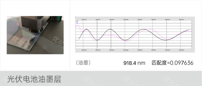
Photovoltaic cell ink thickness measurement results show
The test results show that the thickness of the ink layer is 918.4 nm, and the matching degree is 0.099636! It can be seen that the light wave is stable during the test process, and the stability of the light wave can make the measurement result more accurate. The Atometrics film thickness measuring instrument uses "deuterium lamp" and "tungsten halogen lamp", the light intensity is more uniform, the spectrum is more stable, and it can measure single-layer film, multi-layer film, liquid film, air gap layer, rough layer and smooth layer. One machine covers the measurement range of multiple machines.
2. Coating thickness measurement, roughness measurement and topography analysis after laser etching of perovskite cells
A photovoltaic energy company hopes to test the coating thickness, film roughness and 3D topography after laser etching of perovskite solar cells to improve the photoelectric conversion efficiency of solar cells. Based on customer needs, Atometrics selected the AM-7000 series of white light interferometers for testing:
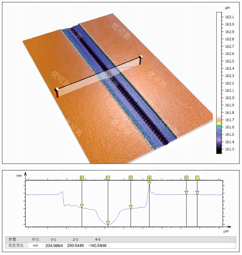
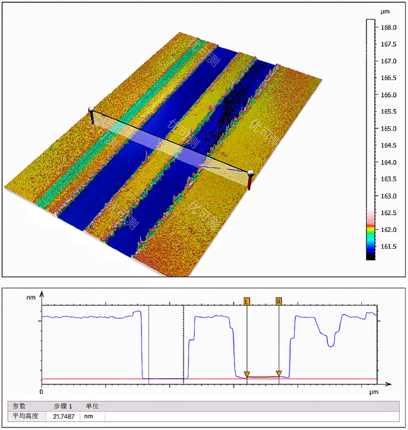
P1 coating thickness measurement

P2 Coating thickness measurement
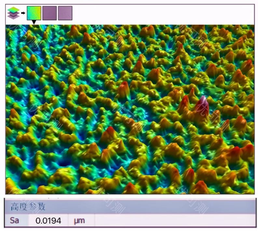
P2 Coating roughness measurement
P3 Topography analysis after laser etching
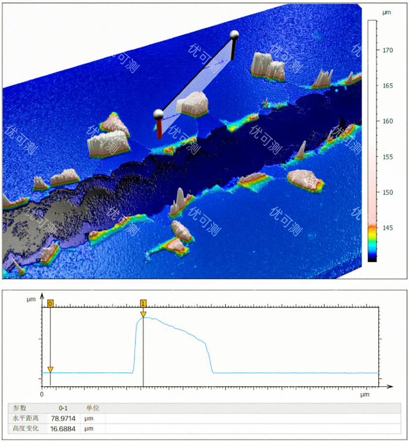
P3 Glitch detection
In summary, the accuracy of the Atometrics white light interferometer reaches the nanometer level. With a large range of high-speed nano-piezoelectric ceramic devices, it can instantly complete up to 5 million point cloud acquisitions, and can quickly, clearly and intuitively detect microscopic three-dimensional morphology. After receiving the test report from Atometrics, the customer said, "The Atometrics white light interferometer can be used for the entire process of our perovskite battery production. It can detect film thickness, roughness, and topography analysis. It is truly a multi-purpose machine!"

Boardstone lntelligent(Shenzhen)Co.,Ltd.
14F,Building C Kaifa Plaza, 7006 Caitian Rd., Futian Dist. Shenzhen
Hotline:400 080 3885
Sales@atometrics.com.cn